 +7 (495) 785-95-25
 +7 (495) 785-95-14
 sale@lcard.ru
 English version
Меню

+7 (495) 785-95-25
sale@lcard.ru
sale@lcard.ru

Стоимость от 119 000 руб.
В наличии
Преимущества

групповая гальваническая развязка всех входов и выходов увеличивает помехозащищенность и надежность систем
широкий диапазон поддерживаемых операционных систем ПК
поставляется с бесплатным программным обеспечением
разработано и серийно выпускается в России

| АЦП | |||||||||||||||||||||||||||||||||||||||||||||||||||||
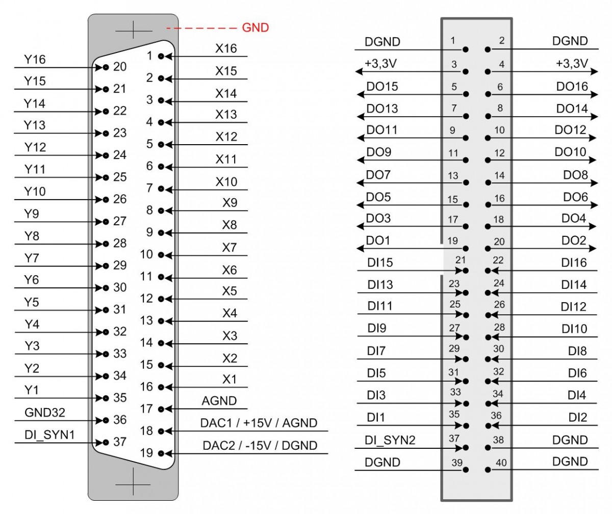
| Количество каналов | 16 дифференциальных или 32 с "общей землей" | ||||||||||||||||||||||||||||||||||||||||||||||||||||
| Разрядность АЦП | 16 бит | ||||||||||||||||||||||||||||||||||||||||||||||||||||
| Поддиапазоны измерения входного сигнала | ±10 В, ±5 В, ±2 В, ±1 В, ±0,5 В, ±0,2 В | ||||||||||||||||||||||||||||||||||||||||||||||||||||
| Максимальная частота преобразования АЦП | 2 МГц (1,5 МГц при синхронизации частоты преобразования от соседней платы L-502) |
||||||||||||||||||||||||||||||||||||||||||||||||||||
| Устойчивость к перегрузкам входным измерительным сигналом напряжения постоянного тока | ±15 В | ||||||||||||||||||||||||||||||||||||||||||||||||||||
| Синхронизация |
|
||||||||||||||||||||||||||||||||||||||||||||||||||||
| Собственнй входной шум АЦП при закороченном входе в зависимости от поддиапазона АЦП и коэффициента усреднения отсчётов (Куср) по каждому каналу. |
|
||||||||||||||||||||||||||||||||||||||||||||||||||||
| Межканальное прохождение АЦП, дБ |
|
||||||||||||||||||||||||||||||||||||||||||||||||||||
| Цифровой сигнальный процессор (L-502-P-G, L-502-P-G-D, L-502-P-G-D-I) | |||||||||||||||||||||||||||||||||||||||||||||||||||||
| Тип | Blackfin ADSP-BF523 | ||||||||||||||||||||||||||||||||||||||||||||||||||||
| Тактовая частота | 530 МГц | ||||||||||||||||||||||||||||||||||||||||||||||||||||
| ОЗУ | 32 Мбайт (SDRAM, 16 бит; 132,5 МГц) | ||||||||||||||||||||||||||||||||||||||||||||||||||||
| Интерфейс компьютера с ADSP-BF523 | Независимый, через HOST DMA процессора ADSP-BF523 | ||||||||||||||||||||||||||||||||||||||||||||||||||||
| Основной интерфейс работы с периферией (АЦП, ЦАП, цифровой ввод/вывод) | SPORT0, >120 Мбит/c, дуплекс | ||||||||||||||||||||||||||||||||||||||||||||||||||||
| Гальваническая развязка (L-502-X-G, L-502-X-G-D, L-502-P-G, L-502-P-G-D, L-502-P-G-D-I ) | |||||||||||||||||||||||||||||||||||||||||||||||||||||
| Граница гальванической развязки | Между всеми цепями, выходящими на контакты сигнальных разъёмов, и цепями ПК. Металлический корпус разъема DRB-37М гальванически не развязан от ПК. | ||||||||||||||||||||||||||||||||||||||||||||||||||||
| Испытательное напряжение гальванической развязки | 500 В, 50 Гц в течение 1 мин. | ||||||||||||||||||||||||||||||||||||||||||||||||||||
| Модификации L-502, в которых присутствует гальваническая развязка | L-502-P-G, L-502-P-G-D, L-502-X-G, L-502-X-G-D | ||||||||||||||||||||||||||||||||||||||||||||||||||||
| ЦАП (L-502-X-X-D, L-502-X-G-D, L-502-P-G-D, L-502-P-G-D-I) | |||||||||||||||||||||||||||||||||||||||||||||||||||||
| Количество выходов напряжения с общей землёй | 2 | ||||||||||||||||||||||||||||||||||||||||||||||||||||
| Тип ЦАП | Инструментальный | ||||||||||||||||||||||||||||||||||||||||||||||||||||
| Частота вывода в синхронном режиме | 1 МГц на каждый канал | ||||||||||||||||||||||||||||||||||||||||||||||||||||
| Режимы вывода | Синхронный (потоковый) или асинхронный - воспроизведение напряжения постоянного и переменного тока | ||||||||||||||||||||||||||||||||||||||||||||||||||||
| Выходной диапазон | ±5 В | ||||||||||||||||||||||||||||||||||||||||||||||||||||
| Рабочий выходной ток | Не более 10 мА | ||||||||||||||||||||||||||||||||||||||||||||||||||||
| Цифровые входы | |||||||||||||||||||||||||||||||||||||||||||||||||||||
| Общее количество цифровых входов общего назначения | 18 (из них два могут быть использованы для синхронизации) | ||||||||||||||||||||||||||||||||||||||||||||||||||||
| Режимы ввода данных | Синхронный, асинхронный | ||||||||||||||||||||||||||||||||||||||||||||||||||||
| Программное управление включением резисторных подтяжек к высокому логическому уровню | Присутствует | ||||||||||||||||||||||||||||||||||||||||||||||||||||
| Максимальная скорость в синхронном режиме | 2 МГц | ||||||||||||||||||||||||||||||||||||||||||||||||||||
| Диапазон напряжений на цифровых входах |
-0,2...+0,6 В («логический ноль») +2,4...+5,0 В («логическая единица»). |
||||||||||||||||||||||||||||||||||||||||||||||||||||
| Высокоимпедансное состояние при выключенном питании | Присутствует | ||||||||||||||||||||||||||||||||||||||||||||||||||||
| Сопротивление резисторной подтяжки | 2,2 кОм относительно +3,3 В (резисторные подтяжки программно включаемые для групп входов) | ||||||||||||||||||||||||||||||||||||||||||||||||||||
| Цифровые выходы | |||||||||||||||||||||||||||||||||||||||||||||||||||||
| Общее количество цифровых выходов | 16 | ||||||||||||||||||||||||||||||||||||||||||||||||||||
| Управление третьим состоянием выходов | Присутствует | ||||||||||||||||||||||||||||||||||||||||||||||||||||
| Режимы вывода данных | Синхронный, асинхронный | ||||||||||||||||||||||||||||||||||||||||||||||||||||
| Максимальная скорость в синхронном режиме | 1 Мслов/c | ||||||||||||||||||||||||||||||||||||||||||||||||||||
| Тип логики | TTL-совместимая | ||||||||||||||||||||||||||||||||||||||||||||||||||||
| Диапазон напряжений на цифровых выходах |
0...+0,4 В («логический ноль») Не менее 2,4 В («логическая единица»), выходные логические элементы с напряжением питания 3,3 В. |
||||||||||||||||||||||||||||||||||||||||||||||||||||
| Рабочий ток выхода |
Не более 8 мА |
||||||||||||||||||||||||||||||||||||||||||||||||||||
| Выходное сопротивление, типичное значение | 110 Ом | ||||||||||||||||||||||||||||||||||||||||||||||||||||
| Максимальный ток утечки в рабочем режиме в высокоимпедансном состоянии | ±1 мкА | ||||||||||||||||||||||||||||||||||||||||||||||||||||
| Высокоимпедансное состояние при выключенном питании | Отсутствует | ||||||||||||||||||||||||||||||||||||||||||||||||||||
| Межмодульная синхронизация | |||||||||||||||||||||||||||||||||||||||||||||||||||||
| Топология многомодульных соединений по линиям синхронизации | Последовательная (внутри одного системного блока ПК) | ||||||||||||||||||||||||||||||||||||||||||||||||||||
| Максимальное количество синхронизируемых модулей L-502 по последовательной схеме синхронизации | Равно количеству PCIe слотов в материнской плате ПК | ||||||||||||||||||||||||||||||||||||||||||||||||||||
| Максимальная длина кабеля межмодульной синхронизации | 40 мм (только до L-502 в соседнем слоте PCIe) | ||||||||||||||||||||||||||||||||||||||||||||||||||||
| Количество линий межмодульной синхронизации | 2 витые пары | ||||||||||||||||||||||||||||||||||||||||||||||||||||
| Интерфейс с комьютером | |||||||||||||||||||||||||||||||||||||||||||||||||||||
| Стандарт | PCIe x1 rev. 1.0 (плата совместима со слотом PCI Express материнской платы любой пропускной способности: x1, x2, x4, x8, x12, x16, x32). | ||||||||||||||||||||||||||||||||||||||||||||||||||||
| Максимальная скорость передачи данных по PCIe | 200 Мбайт/с, дуплекс (физическая пропускная способность PCIe-контроллера) | ||||||||||||||||||||||||||||||||||||||||||||||||||||
| Разрядность программного слова данных L-502 на PCIe | 32 бит | ||||||||||||||||||||||||||||||||||||||||||||||||||||
| Поддержка DMA в режиме BUS MASTER на PCIe | Имеется | ||||||||||||||||||||||||||||||||||||||||||||||||||||
| Конструктивные характеристики | |||||||||||||||||||||||||||||||||||||||||||||||||||||
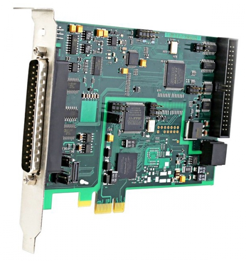
| Конструктив | PCI Express CARD x1 стандартной высоты, с кронштейном, менее, чем половинной длины (HALF LENGTH), в соответствии с PCI Express Card Electromechanical Specification rev.2.0. Требует одного посадочного места PCI Express. |
||||||||||||||||||||||||||||||||||||||||||||||||||||
| Габаритные размеры | Не более 150 x 122 x 22 мм | ||||||||||||||||||||||||||||||||||||||||||||||||||||
| Масса | Не более 0,15 кг | ||||||||||||||||||||||||||||||||||||||||||||||||||||
| Питание внешних цепей | |||||||||||||||||||||||||||||||||||||||||||||||||||||
| Выходы питания внешних аналоговых и цифровых цепей | +15 В, -15 В, +3,3 В. Максимальные токи, снимаемые с выходов, выбираются по критерию непревышения максимальной мощности нагрузки по методике, изложенной в руководстве. | ||||||||||||||||||||||||||||||||||||||||||||||||||||
| Максимальная мощность нагрузки, снимаемой со всех выходов L-502 |
0,4 Вт (L-502-X-X-D, L-502-X-G-D, L-502-P-G-D, L-502-P-G-D-I) 0,8 Вт (L-502-X-X, L-502-X-G, L-502-P-G) |
||||||||||||||||||||||||||||||||||||||||||||||||||||
|
АЦП |
|
| Диапазон измерений напряжения постоянного тока | От -10 до +10 В |
|
Пределы допускаемой приведенной (к верхнему значению предела
измерений) основной погрешности измерений напряжения постоянного
тока для пределов:
– 10; 5 и 2 В
– 1 В
– 0,5 В
– 0,2 В
|
±0,05 %
±0,07 %
±0,1 %
±0,2 %
|
| Диапазон измерений напряжения переменного тока в диапазоне частот от 0,01 до 999 кГц |
От 0,2 мВ до 7 В |
| Пределы допускаемой относительной основной погрешности измерений напряжения переменного тока ** |
 XAC – предел измерений напряжения переменного тока; X – значение измеряемого напряжения переменного тока |
| Входное сопротивление постоянному току в одноканальном режиме работы |
Не менее 20 МОм |
| Коэффициент подавления синфазных помех | Не менее 70 дБ |
| Пределы допускаемой относительной основной погрешности частоты преобразований АЦП | ±0,005 % |
| ЦАП (L-502-X-X-D, L-502-X-G-D, L-502-P-G-D, L-502-P-G-D-I) | |
| Диапазон воспроизведений напряжения постоянного тока | От -5 до +5 В |
| Пределы допускаемой приведенной (к верхней границе диапазона воспроизведений) основной погрешности воспроизведений напряжения постоянного тока | ±0,3 % |
| Диапазон воспроизведений напряжения переменного тока синусоидальной формы в диапазоне частот от 0,01 до 300 кГц | От 1 мВ до 3,5 В |
| Пределы допускаемой относительной основной погрешности воспроизведений напряжения переменного тока 2) | XAC – конечное значение диапазона воспроизведений напряжения переменного тока, XAC = 3,5 В; X – значение воспроизводимого напряжения переменного тока |
| Пределы допускаемой относительной основной погрешности воспроизведений частоты переменного тока | ±0,005 % |
|
Условия эксплуатации |
|
|
Нормальные условия применения |
|
| Температура окружающей среды | 20±5 °С |
| Относительная влажность | От 30 до 80 % |
| Атмосферное давление | От 84 до 106 кПа |
|
Рабочие условия применения L-502-X-X, L-502-X-X-D, L-502-X-G, L-502-X-G-D, L-502-P-G, L-502-P-G-D |
|
| Температура окружающей среды | От +5 до +55 °С |
| Относительная влажность при температуре окружающей среды 25 °С | До 90 % |
| Атмосферное давление | От 70 до 106,7 кПа |
|
Рабочие условия применения L-502-P-G-D-I |
|
| Температура окружающей среды | От -40 до +60 °С |
| Относительная влажность при температуре окружающей среды 30 °С | До 90 % |
| Атмосферное давление | От 70 до 106,7 кПа |
| Пределы допускаемых дополнительных погрешностей измерений напряжения постоянного и переменного тока, воспроизведений напряжения постоянного и переменного тока, частоты переменного тока, частоты преобразований АЦП от изменения температуры окружающей среды в диапазоне рабочих температур, на каждые 10 ºC, в долях от пределов допускаемой основной погрешности | 0,5 |
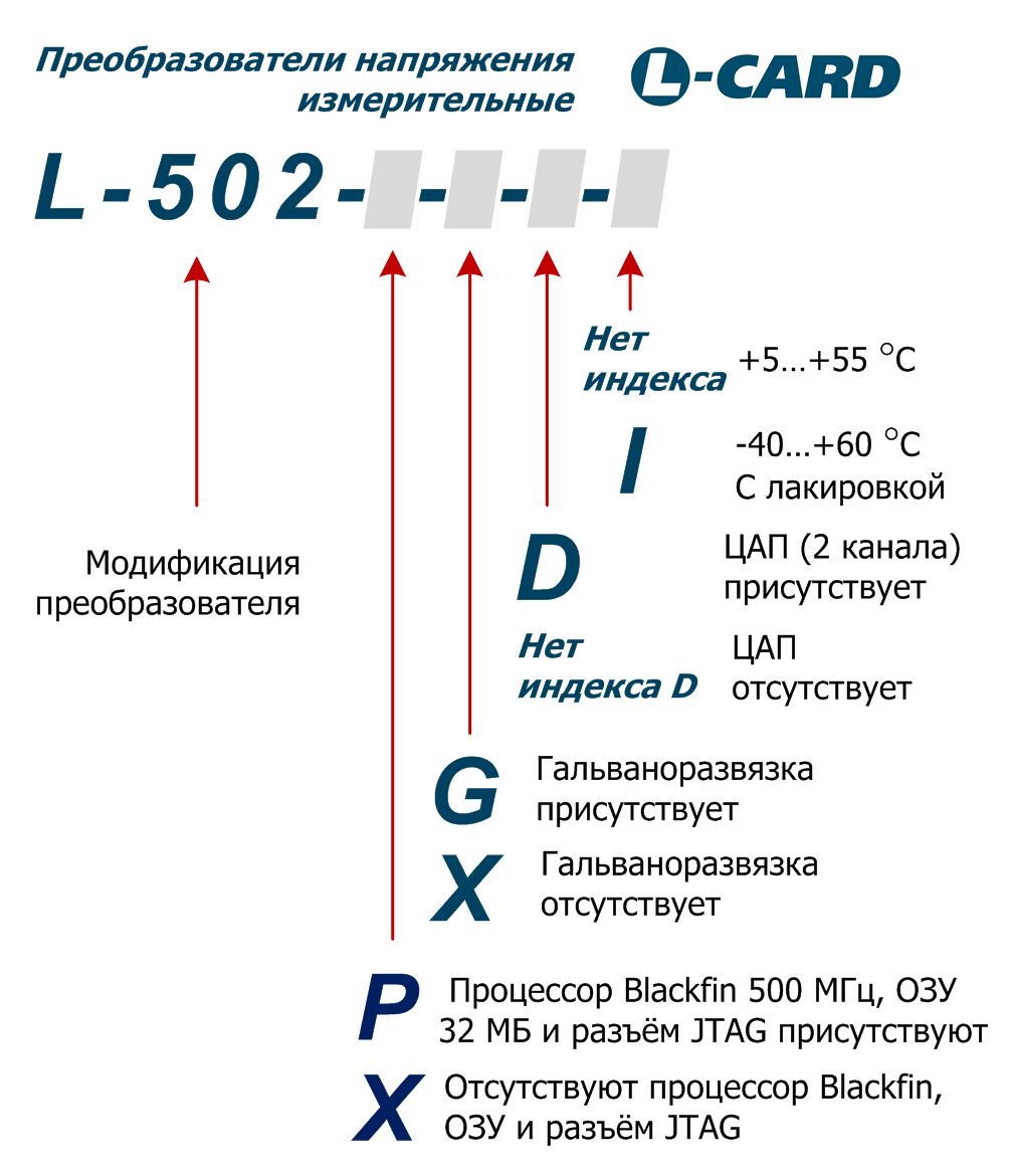
Примечание по технически возможным модификациям L-502: При заказе от 40-50 шт. возможен выпуск чисто цифровой модификациии L-502 без аналогового ввода-вывода АЦП/ЦАП по сниженной цене. О заинтересованности в подобной модификации L-502 сообщайте в отдел продаж L-Card.
| L-502-X-G | Цена 119000.00 руб./шт. Минимальная партия для заказа 20 шт. |
| Плата без ЦАП, с гальваноразвязкой, без DSP | |
| L-502-X-G-D | Цена 124000.00 руб./шт. Минимальная партия для заказа 20 шт. |
| Плата с ЦАП, с гальваноразвязкой, без DSP | |
| L-502-P-G-D | Цена 132000.00 руб. |
| Плата с ЦАП, с гальваноразвязкой, с DSP | |
| L-502-P-G-D-I-m | Цена 142000.00 руб./шт. Минимальная партия для заказа 20 шт. |
| Плата с ЦАП, с гальваноразвязкой, с DSP, индустриальная, с поверкой | |
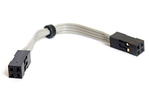
Кабель цифровых сигналов
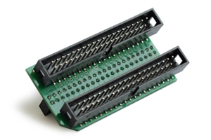
Переходник цифрового разъема
плат L-xxx
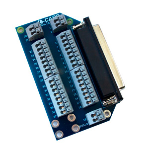
Плата клеммников на 37 контактнов
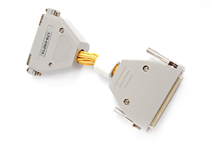
Синфазный помехоподавляющий фильтр
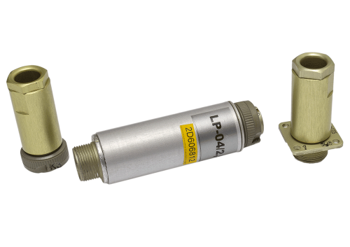
Универсальный предусилитель милливольтовых сигналов LP-04-M
Кабель синхронизации L-502-SYNC
Декларация о соответствии Техническим регламентам Таможенного Союза (ТР ТС)
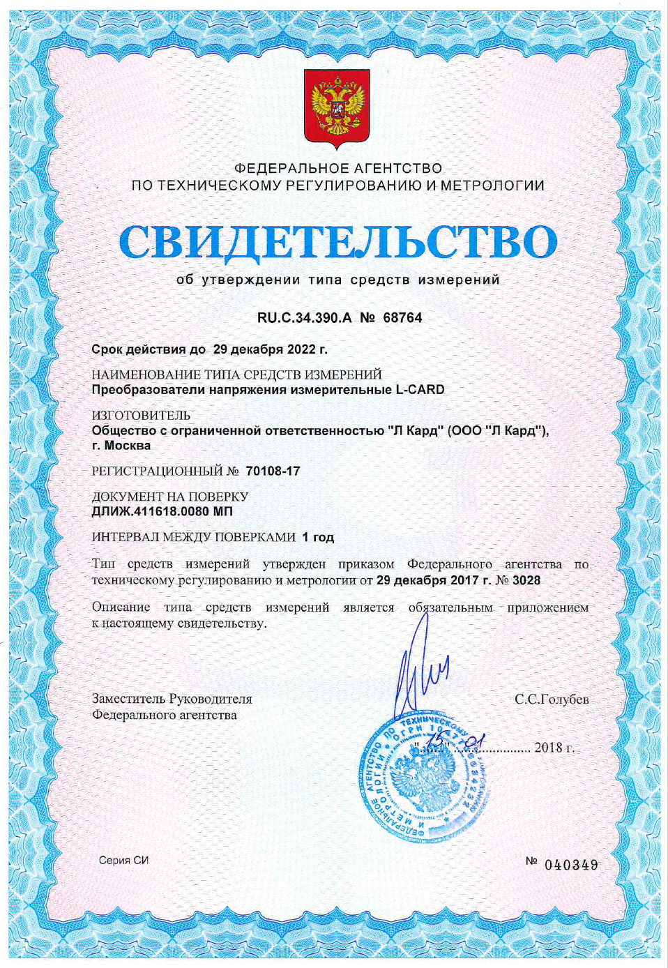
Свидетельство об утверждении типа средств измерений. Преобразователи напряжения измерительные L-CARD.
Модификации преобразователей:
Приказ о продлении действия 'Свидетельства об утверждении типа средств измерений' до 29.12.2027.
Преобразователи напряжения измерительные L-CARD: E14-140, E14-440, E20-10, E-502 и L-502.
Методика поверки.
3D модель модуля L-502 с установленным переходником PBD2BH в формате PDF.
Для надлежащего отображение данного документа в используемой программе просмотра PDF файлов необходимо в её настройках включить поддержку 3D.
Например, для программы 'Adobe Acrobat Reader' это делается так.
3D модель модуля L-502 с установленным переходником PBD2BH в формате STP.
3D модель модуля L-502 в формате PDF.
Для надлежащего отображение данного документа в используемой программе просмотра PDF файлов необходимо в её настройках включить поддержку 3D.
Например, для программы 'Adobe Acrobat Reader' это делается так.
3D модель модуля L-502 в формате STP.
L-502 Преобразователь напряжения измерительный.
Инструкция по первоначальной настройке.
Руководство пользователя PCI-Express платы L-502 в формате Adobe Acrobat.
Преобразователи напряжения измерительные L-CARD: E14-140, E14-440, E20-10, E-502 и L-502.
Руководство по эксплуатации.
Руководство программиста для модулей L502 и E502 в формате Adobe Acrobat.
Низкоуровневое руководство программиста для модулей L502 и E502.
Программный комплекс "L Card Measurement Studio" для проведения измерительных экспериментов с использованием оборудования "Л Кард". Версия 1.4.5.
Без приобретения ключа лицензии работает в демонстрационном режиме.
Описание программы.
Список изменений.
История изменений в версиях программного комплекса "L Card Measurement Studio".
Инструкция по установке программного комплекса "L Card Measurement Studio".
Инструкция по эксплуатации программного комплекса "L Card Measurement Studio".
Набор утилит для поверки изделий E-502 и L-502 под ОС Windows'XP/7/8.x/10/11.
Внимательно читаем Readme файл.
Использование открытых репозиториев исходных кодов
"Л Кард" на bitbucket.org
Использование внешних репозиториев "Л Кард" для
дистрибутивов Linux.
Проект "Л Кард" для распространения пакетов под различные дистрибутивы Linux с использованием Open Build Service.
OPC-сервер для модулей сбора данных "Л Кард" и крейтовой системы LTR. Версия 1.1.4.
Руководство: http://www.lcard.ru/download/lcard-opc.pdf.
Без приобретения лицензии работает в демонстрационном режиме.
L-Card L502/E502 SDK. Версия 1.1.24. Включает в себя драйвер, библиотеки, файлы для разработки программ и примеры программирования для модулей L502 и E502 фирмы ООО "Л Кард" под ОС Windows (поддерживаются версии Windows, начиная с Windows XP SP3 и выше, включая 64-битные версии).
Демонстрационная программа для модулей E-502 и L-502
LGraph2 - многофункциональная программа самописец-визуализатор под Windows'XP/7/8.x/10. Версия 2.36.2. Возможность одновременной визуализации и регистрации данных с АЦП L-502, L-780M, L-783, L-791, L-761, E-502, E14-140, E14-140M, E14-440, E-154, E20-10, LTR11, LTR114, LTR27, LTR212, LTR216, LTR22, LTR24, LTR25, LTR51, L-264, L-305, L-1250. Для работы программы требуется предварительно установить подписанные драйвера LComp и службу ltrd c графическим интерфейсом к ней LTR Manager.
История изменений и дополнений в версиях программы LGraph2.
Руководство пользователя программы LGraph2.
Руководство пользователя по разработке плагинов для программы LGraph2.
Руководство программиста для PCI-Express платы L-502 в формате Adobe Acrobat.
L-Card PCI-Express SDK. Включает в себя драйвер,
библиотеки, файлы для разработки программ и примеры программирования
для модулей фирмы ООО "Л Кард" с интерфейсом PCI-Express (модуль L502)
под ОС Windows (поддерживаются версии Windows, начиная с Windows 2000 и
выше, включая 64-битные версии). Версия 1.0.6
Аппаратное описание, назначение и подключение сигналов приведены в Руководстве пользователя.
Адрес: 117105, Москва, Варшавское шоссе, д. 5, корп. 4, стр. 2
Многоканальный телефон:
+7 (495) 785-95-25
Факс: +7 (495) 785-95-14
Отдел продаж: sale@lcard.ru
Техническая поддержка: support@lcard.ru
Время работы: с 9-00 до 19-00 мск

 скачать презентацию
 скачать каталог продукции
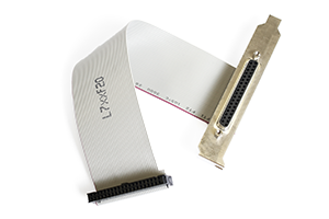
